(China (Mainland))

Product Summary
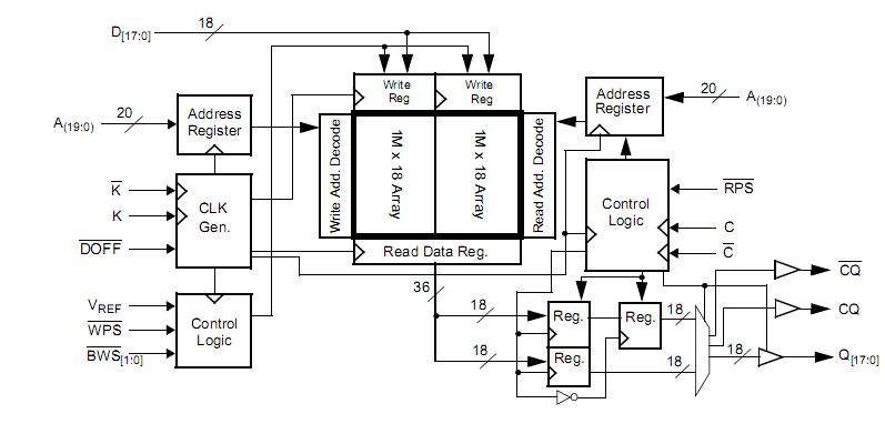
The CY7C1412BV18-200BZI is a 1.8V Synchronous Pipelined SRAM. It is equipped with QDR-II architecture. QDR-II architecture consists of two separate ports: the read port and the write port to access the memory array. The CY7C1412BV18-200BZI operates with a read latency of one and half cycles when DOFF pin is tied HIGH. When DOFF pin is set LOW or connected to VSS then the device behaves in QDR-I mode with a read latency of one clock cycle. The CY7C1412BV18-200BZI is organized internally as two arrays of 1M x 18. Accesses are completed in a burst of two sequential 18-bit data words.
Parametrics
CY7C1412BV18-200BZI absolute maximum ratings: (1)Storage Temperature:–65℃ to +150℃; (2)Ambient Temperature with Power Applied:–55℃ to +125℃; (3)Supply Voltage on VDD Relative to GND:–0.5V to +2.9V; (4)Supply Voltage on VDDQ Relative to GND:–0.5V to +VDD; (5)DC Applied to Outputs in High-Z:–0.5V to VDDQ + 0.3V; (6)DC Input Voltage:–0.5V to VDD + 0.3V; (7)Current into Outputs (LOW):20 mA; (8)Static Discharge Voltage (MIL-STD-883, M. 3015): > 2001V; (9)Latch-up Current: > 200 mA.
Features
CY7C1412BV18-200BZI features: (1)Separate independent read and write data ports: Supports concurrent transactions; (2)250 MHz clock for high bandwidth; (3)2-word burst on all accesses; (4)Double Data Rate (DDR) interfaces on both read and write ports (data transferred at 500 MHz) at 250 MHz ; (5)Two input clocks (K and K) for precise DDR timing: SRAM uses rising edges only; (6)Two input clocks for output data (C and C) to minimize clock skew and flight time mismatches; (7)Echo clocks (CQ and CQ) simplify data capture in high-speed systems; (8)Single multiplexed address input bus latches address inputs for both read and write ports; (9)Separate port selects for depth expansion; (10)Synchronous internally self-timed writes; (11)QDR-II operates with 1.5 cycle read latency when Delay Lock Loop (DLL) is enabled ; (12)Operates as a QDR-I device with 1 cycle read latency in DLL off mode; (13)Available in x 8, x 9, x 18, and x 36 configurations ; (14)Full data coherency, providing most current data; (15)Core VDD = 1.8V (±0.1V); IO VDDQ = 1.4V to VDD; (16)Available in 165-Ball FBGA package (15 x 17 x 1.4 mm); (17)Offered in both Pb-free and non Pb-free packages; (18)Variable drive HSTL output buffers; (19)JTAG 1149.1 compatible test access port; (20)Delay Lock Loop (DLL) for accurate data placement.
Diagrams
| Image | Part No | Mfg | Description |  |
Pricing (USD) |
Quantity | ||||||||||||
|---|---|---|---|---|---|---|---|---|---|---|---|---|---|---|---|---|---|---|
 |
 CY7C1412BV18-200BZI |
Cypress Semiconductor |
SRAM 2Mx18 QDR-II Burst 2 SRAM |
Data Sheet |
Negotiable |
|
||||||||||||
| Image | Part No | Mfg | Description | |
Pricing (USD) |
Quantity | ||||||||||||
 |
CY7C006 |
Other |
|
Data Sheet |
Negotiable |
|
||||||||||||
|
CY7C006A |
Other |
|
Data Sheet |
Negotiable |
|
||||||||||||
 |
CY7C006A-15AXC |
Cypress Semiconductor |
SRAM 5V 16Kx8 COM Dual Port SRAM |
Data Sheet |
Negotiable |
|
||||||||||||
|
CY7C006A-15AXCT |
Cypress Semiconductor |
SRAM 5V 16Kx8 COM Dual Port SRAM |
Data Sheet |
Negotiable |
|
||||||||||||
 |
CY7C006A-20AC |
|
IC SRAM 16KX8 DUAL 64LQFP |
Data Sheet |
Negotiable |
|
||||||||||||
|
CY7C006A-20AXC |
Cypress Semiconductor |
SRAM 5V 16Kx8 COM Dual Port SRAM |
Data Sheet |
|
|
||||||||||||