(China (Mainland))

Product Summary
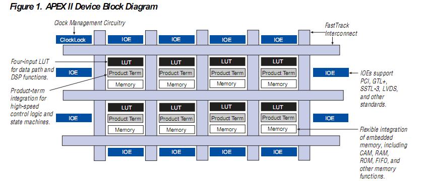
The EP2A15F672C9 is a Programmable logic device (PLD) manufactured using a 0.15-um all-layer copper-metal fabrication process (up to eight layers of metal). Flexible-LVDS pins located in regular user I/O banks offer additional differential support, increasing the total device bandwidth. This circuitry, together with enhanced IOEs and support for numerous I/O standards, allows the EP2A15F672C9 to meet high-speed interface requirements. The EP2A15F672C9 also includes other high-performance features such as bidirectional dual-port RAM, CAM, general-purpose PLLs, and numerous global clocks.
Parametrics
EP2A15F672C9 absolute maximum ratings: (1)Supply voltage:–0.5 to 4.6 V; (2)DC input voltage:–0.5 to 4.6 V; (3)DC output current, per pin: –25 to 25 mA; (4)Storage temperature No bias:–65 to 150℃; (5)Ambient temperature:–65 to 135℃; (6)Junction temperature:135℃.
Features
EP2A15F672C9 features: (1)1.5-V supply voltage; (2)Copper interconnect reduces power consumption; (3)MultiVoltTM I/O support for 1.5-V, 1.8-V, 2.5-V, and 3.3-V interfaces; (4)ESBs offer programmable power-saving mode; (5)1,900,000 to 5,250,000 maximum system gates; (6)Up to 67,200 logic elements (LEs); (7)Up to 1,146,880 RAM bits that can be used without reducing available logic; (8)High-performance, low-power copper interconnect; (9)Fast parallel byte-wide synchronous device configuration; (10)Look-up table (LUT) logic available for register-intensive functions; (11)1-gigabit per second (Gbps) True-LVDSTM, LVPECL, pseudo current mode logic (PCML), and HyperTransportTM interface; (12)Clock-data synchronization (CDS) in True-LVDS interface to correct any fixed clock-to-data skew; (13)Enables common networking and communications bus I/O standards such as RapidIOTM, CSIX, Utopia IV, and POS-PHY Level 4; (14)Support for high-speed external memory interfaces, including zero bus turnaround (ZBT), quad data rate (QDR), and double data rate (DDR) static RAM (SRAM), and single data rate (SDR) and DDR synchronous dynamic RAM (SDRAM); (15)30% to 40% faster design performance than APEXTM 20KE devices on average.
Diagrams
 |
 EP2A25F672C9 |
Other |
|
Data Sheet |
Negotiable |
|
||||||
|
EP2AGX125DF25C4 |
|
IC ARRIA II GX FPGA 125K 572FBGA |
Data Sheet |
|
|
||||||
 |
EP2AGX125DF25C4N |
|
IC ARRIA II GX FPGA 125K 572FBGA |
Data Sheet |
|
|
||||||
|
EP2AGX125DF25C5 |
|
IC ARRIA II GX FPGA 125K 572FBGA |
Data Sheet |
|
|
||||||
|
EP2AGX125DF25C5N |
|
IC ARRIA II GX FPGA 125K 572FBGA |
Data Sheet |
|
|
||||||
|
EP2AGX125DF25C6 |
|
IC ARRIA II GX FPGA 125K 572FBGA |
Data Sheet |
|
|
||||||