(China (Mainland))

Product Summary
The Altera EPF6016QC240-3 programmable logic device (PLD) provides a low-cost alternative to high-volume gate array designs. EPF6016QC240-3 device is based on the OptiFLEX architecture, which minimizes die size while maintaining high performance and routability. The device has reconfigurable SRAM elements, which give designers the flexibility to quickly change their designs during prototyping and design testing. Designers can also change functionality during operation via in-circuit reconfiguration. EPF6016QC208-3N device is reprogrammable, and it is 100% tested prior to shipment. As a result, designers are not required to generate test vectors for fault coverage purposes, allowing them to focus on simulation and design verification. In addition, the designer does not need to manage inventories of different gate array designs. EPF6016QC240-3 device is configured on the board for the specific functionality required.
Parametrics
EPF6016QC240-3 absolute maximum ratings: (1)VCC Supply voltage With respect to ground: -2.0 to 7.0 V; (2)VI DC input voltage: -2.0 to 7.0 V; (3)IOUT DC output current, per pin: -25 to 25 mA; (4)TSTG Storage temperature No bias: -65 to 150 ℃; (5)TAMB Ambient temperature Under bias: -65 to 135 ℃; (6)TJ Junction temperature PQFP, TQFP, and BGA packages: 135 ℃.
Features
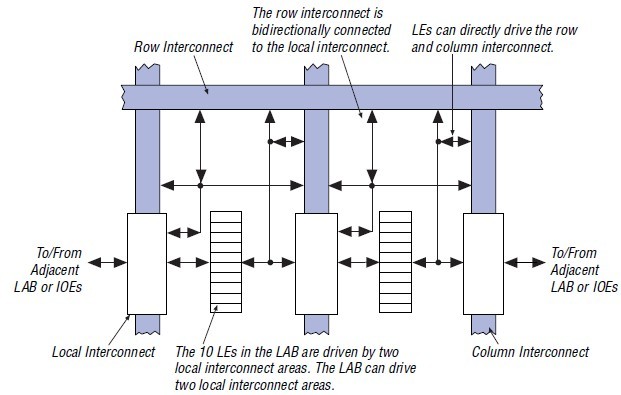
EPF6016QC240-3 features: (1)Provides an ideal low-cost, programmable alternative to highvolume gate array applications and allows fast design changes during prototyping or design testing; (2)Register-rich, look-up table- (LUT-) based architecture; (3)ptiFLEX architecture that increases device area efficiency; (4)Typical gates ranging from 5,000 to 24,000 gates; (5)Built-in low-skew clock distribution tree; (6)100% functional testing of all devices; test vectors or scan chains are not required; (7)In-circuit reconfigurability (ICR) via external configuration device or intelligent controller; (8)5.0-V devices are fully compliant with peripheral component; (9)interconnect Special Interest Group (PCI SIG) PCI Local Bus Specification, Revision 2.2; (10)Built-in Joint Test Action Group (JTAG) boundary-scan test (BST) circuitry compliant with IEEE Std. 1149.1-1990, available without consuming additional device logic; (11)MultiVoltTM I/O interface operation, allowing a device to bridge between systems operating at different voltages; (12)Low power consumption (typical specification less than 0.5 mA in standby mode; (13)3.3-V devices support hot-socketing Software design support and automatic place-and-route provided by Altera development system for Windows-based PCs, Sun SPARCstations, and HP 9000 Series 700/800.
Diagrams
| Image | Part No | Mfg | Description |  |
Pricing (USD) |
Quantity | ||||||
|---|---|---|---|---|---|---|---|---|---|---|---|---|
 |
 EPF6016QC240-3 |
|
IC FLEX 6000 FPGA 16K 240-PQFP |
Data Sheet |
|
|
||||||
|
EPF6016QC240-3N |
|
IC FLEX 6000 FPGA 16K 240-PQFP |
Data Sheet |
|
|
||||||