(China (Mainland))

Product Summary
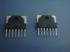
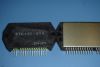
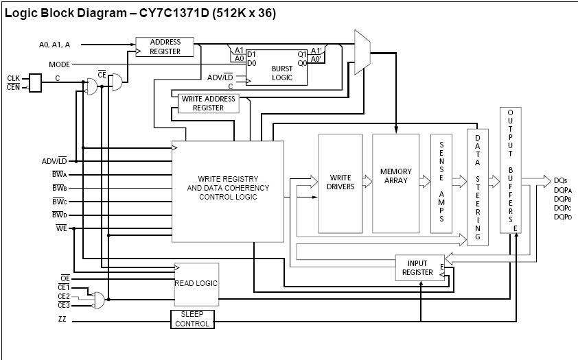
The CY7C1371D-100AXC is a 3.3V, 512K x 36/1Mbit x 18 Synchronous Flow-through Burst SRAM. The CY7C1371D-100AXC is designed specifically to support unlimited true back-to-back Read/Write operations without the insertion of wait states. The CY7C1371D-100AXC is equipped with the advanced No Bus Latency (NoBL) logic required to enable consecutive Read/Write operations with data being transferred on every clock cycle. This feature dramatically improves the throughput of data through the SRAM, especially in systems that require frequent Write-Read transitions.
Parametrics
CY7C1371D-100AXC absolute maximum ratings: (1)Storage Temperature: –65℃ to +150℃; (2)Ambient Temperature with Power Applied: –55℃ to +125℃; (3)Supply Voltage on VDD Relative to GND:–0.5V to +4.6V; (4)DC Voltage Applied to Outputs in Tri-State:–0.5V to VDDQ + 0.5V; (5)DC Input Voltage:–0.5V to VDD + 0.5V; (6)Current into Outputs (LOW):20mA; (7)Static Discharge Voltage (per MIL-STD-883, Method 3015): >2001V; (8)Latch-up Current: >200mA.
Features
CY7C1371D-100AXC features: (1)No Bus Latency. (NoBL.) architecture eliminates dead cycles between write and read cycles; (2)Can support up to 133-MHz bus operations with zero wait states; (3)Data is transferred on every clock; (4)Pin-compatible and functionally equivalent to ZBT devices; (5)Internally self-timed output buffer control to eliminate the need to use OE; (6)Registered inputs for flow-through operation; (7)Byte Write capability; (8)3.3V/2.5V I/O power supply; (9)Fast clock-to-output times: 6.5 ns (for 133-MHz device), 8.5 ns (for 100-MHz device); (10)Clock Enable (CEN) pin to enable clock and suspend operation; (11)Synchronous self-timed writes; (12)Asynchronous Output Enable; (13)Offered in JEDEC-standard lead-free 100 TQFP, 119-ball BGA and 165-ball fBGA packages; (14)Three chip enables for simple depth expansion; (15)Automatic Power-down feature available using ZZ mode or CE deselect; (16)JTAG boundary scan for BGA and fBGA packages; (17)Burst Capability—linear or interleaved burst order; (18)Low standby power.
Diagrams
| Image | Part No | Mfg | Description |  |
Pricing (USD) |
Quantity | ||||||||||||
|---|---|---|---|---|---|---|---|---|---|---|---|---|---|---|---|---|---|---|
 |
 CY7C1371D-100AXC |
Cypress Semiconductor |
SRAM 512Kx36 3.3V NoBL Sync FT SRAM COM |
Data Sheet |
|
|
||||||||||||
|
CY7C1371D-100AXCT |
Cypress Semiconductor |
SRAM 512Kx36 3.3V NoBL Sync FT SRAM COM |
Data Sheet |
|
|
||||||||||||