Product Summary
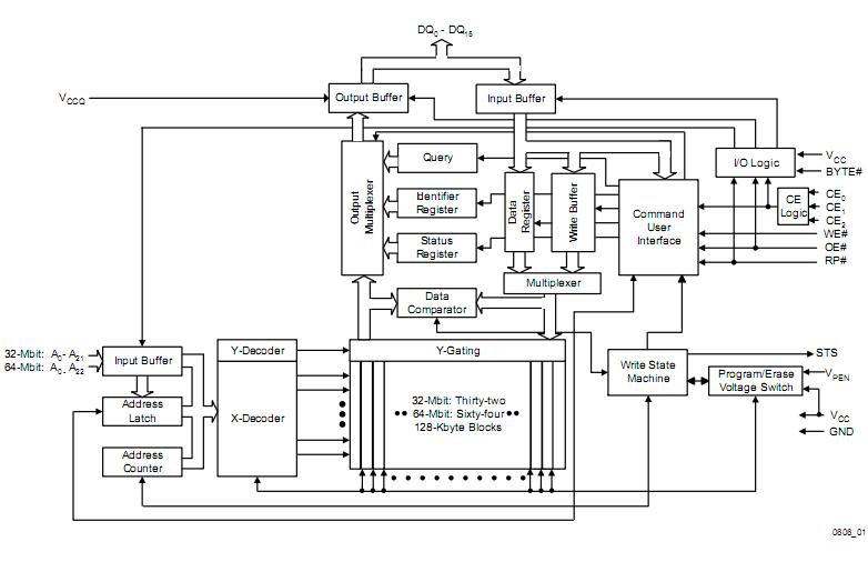
The G28F640J5150 is an Intel StrataFlash memory. It contains high-density memories organized as 8 Mbytes or 4 Mwords (64-Mbit) and 4 Mbytes or 2 Mwords (32-Mbit). Thes G28F640J5150 can be accessed as 8- or 16-bit words. The G28F640J5150 incorporates a Write Buffer of 32 bytes (16 words) to allow optimum programming performance. By using the Write Buffer, data is programmed in buffer increments. This feature can improve system program performance by up to 20 times over non Write Buffer writes.
Parametrics
G28F640J5150 absolute maximum ratings: (1)Commercial Operating Temperature: During Read, Block Erase, Program, and Lock-Bit Configuration:0℃ to +70℃, Temperature under Bias:–10℃ to +80℃, Storage Temperature:–65℃ to +125℃; (2)Voltage On Any Pin (except RP#):–2.0V to +7.0V; (3)RP# Voltage with Respect to GND during Lock-Bit Configuration Operations–2.0V to +14.0V; (4)Output Short Circuit Current:100 mA.
Features
G28F640J5150 features: (1)High-Density Symmetrically-Blocked Architecture: 64 128-Kbyte Erase Blocks (64 M), 32 128-Kbyte Erase Blocks (32 M); (2)5 V VCC Operation:2.7 V I/O Capable; (3)Configurable x8 or x16 I/O; (4)120 ns Read Access Time (32 M), 150 ns Read Access Time (64 M); (5)Enhanced Data Protection Features: Absolute Protection with VPEN = GND, Flexible Block Locking, Block Erase/Program Lockout during Power Transitions; (6)Industry-Standard Packaging: μBGA* Package, SSOP and TSOP Packages (32 M); (7)Cross-Compatible Command Support: Intel Basic Command Set, Common Flash Interface, Scaleable Command Set; (8)32-Byte Write Buffer: 6 μs per Byte Effective Programming Time; (9)640,000 Total Erase Cycles (64 M), 320,000 Total Erase Cycles (32 M), 10,000 Erase Cycles per Block; (10)Automation Suspend Options:Block Erase Suspend to Read, Block Erase Suspend to Program; (11)System Performance Enhancements:STS Status Output; (12)Intel StrataFlash Memory Flash Technology.
Diagrams

 (China (Mainland))


