Product Summary
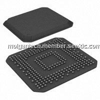
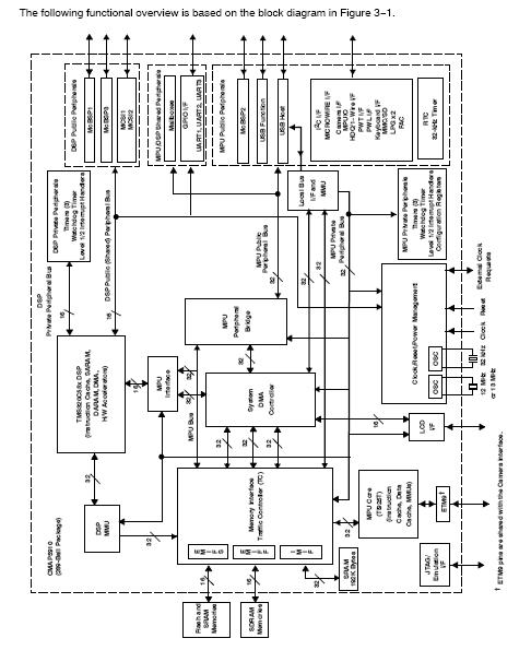
The OMAP5910JGZG2 is a highly integrated hardware and software platform, designed to meet the application processing needs of next-generation embedded devices. The OMAP5910JGZG2 provides benefits of both DSP and RISC technologies, incorporating a TMS320C55x DSP core and a high-performance TI925T ARM core. The applications of the OMAP5910JGZG2 include Applications processing devices, Mobile communications, Video and image processing, advanced speech applications, audio processing, Graphics and video acceleration, generalized web access, Data processing.
Parametrics
OMAP5910JGZG2 absolute maximum ratings: (1)Supply voltage range (core), CVDD,CVDD1/2/3/4/A: -0.3 V to 1.8 V; (2)Supply voltage range (I/O), DVDD1/2/3/4/5: -0.3 V to 4 V; (3)Input voltage range, VI (12-MHz and 32-kHz oscillator): -0.3 V to CVDD + 0.5 V; (4)Input voltage range, VI (standard LVCMOS): -0.3 V to DVDD + 0.5 V; (5)Input voltage range, VI (fail-safe LVCMOS): -0.3 V to 4.5 V; (6)Input voltage range, VI (USB transceivers): -0.3 V to DVDD + 0.5 V; (7)Input voltage range, VI (I2C): -0.3 V to 4.5 V; (8)Output voltage range, VO (standard LVCMOS): -0.3 V to DVDD + 0.5 V; (9)Output voltage range, VO (fail-safe LVCMOS): -0.3 V to 4.5 V; (10)Output voltage range, VO (USB transceivers): -0.3 V to DVDD + 0.5 V; (11)Output voltage range, VO (I2C): -0.3 V to 4.5 V; (12)Operating temperature range, TC: -40℃ to 85℃; (13)Storage temperature range, Tstg: -55℃ to 150℃.
Features
OMAP5910JGZG2 features: (1)Low-Power, High-Performance CMOS Technology; (2)Support 32-Bit and 16-Bit (Thumb. Mode) Instruction Sets; (3)16K-Byte Instruction Cache; (4)8K-Byte Data Cache; (5)Data and Program Memory Management Units (MMUs); (6)Two 64-Entry Translation Look-Aside Buffers (TLBs) for MMUs; (7)17-Word Write Buffer; (8)192K Bytes of Shared Internal SRAM; (9)Memory Traffic Controller (TC); (10)9-Channel System DMA Controller; (11)DSP Memory Management Unit; (12)Endianism Conversion Logic; (13)Digital Phase-Locked Loop (DPLL) for MPU/DSP/TC Clocking Control; (14)DSP Peripherals; (15)TI925T Peripherals; (16)Shared Peripherals; (17)Individual Power-Saving Modes for MPU/DSP/TC; (18)On-Chip Scan-Based Emulation Logic; (19)IEEE Std 1149.1?(JTAG) Boundary Scan Logic; (20)Two 289-Ball Ball Grid Array Package Options (GZG and GDY Suffixes).
Diagrams
| Image | Part No | Mfg | Description |  |
Pricing (USD) |
Quantity | ||||||||||||
|---|---|---|---|---|---|---|---|---|---|---|---|---|---|---|---|---|---|---|
 |
 OMAP5910JGZG2 |
 Texas Instruments |
 Digital Signal Processors & Controllers (DSP, DSC) Applications Proc |
 Data Sheet |

|
|
||||||||||||
| Image | Part No | Mfg | Description |  |
Pricing (USD) |
Quantity | ||||||||||||
 |
 OMAP1623B1ZWE |
 Other |
 |
 Data Sheet |
 Negotiable |
|
||||||||||||
 |
 OMAP3503DCBB |
 Texas Instruments |
 Processors - Application Specialized Applications Proc |
 Data Sheet |
 Negotiable |
|
||||||||||||
 |
 OMAP3503DCBBA |
 Texas Instruments |
 Processors - Application Specialized Applications Proc |
 Data Sheet |
 Negotiable |
|
||||||||||||
 |
 OMAP3503DCBC |
 Texas Instruments |
 Processors - Application Specialized App Processor |
 Data Sheet |
 Negotiable |
|
||||||||||||
 |
 OMAP3503DCBCA |
 Texas Instruments |
 Processors - Application Specialized Applications Proc |
 Data Sheet |
 Negotiable |
|
||||||||||||
 |
 OMAP3503DCUS |
 Texas Instruments |
 Processors - Application Specialized App Processor |
 Data Sheet |
 Negotiable |
|
||||||||||||
 (China (Mainland))

