(China (Mainland))

Product Summary
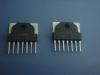
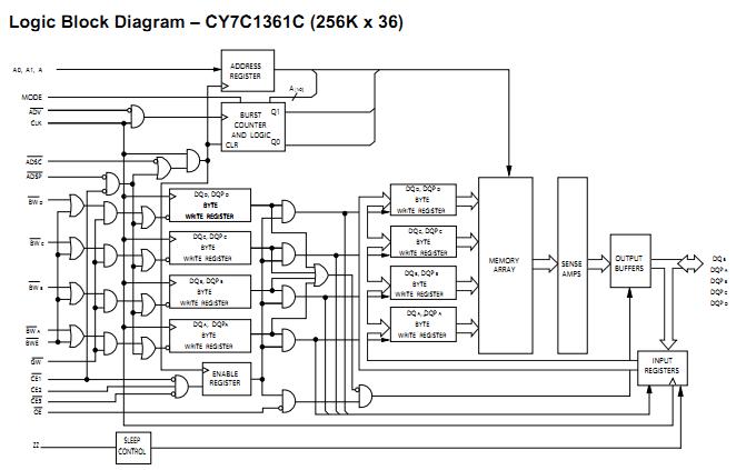
The CY7C1361C-100BGC is a 3.3V, 256K x 36/512K x 18 synchronous flow-through SRAM. The CY7C1361C-100BGC is respectively designed to interface with high speed microprocessors with minimum glue logic. Maximum access delay from clock rise is 6.5 ns (133 MHz version). A 2-bit on-chip counter captures the first address in a burst and increments the address automatically for the rest of the burst access. All synchronous inputs of the CY7C1361C-100BGC are gated by registers controlled by a positive-edge-triggered Clock Input (CLK). The synchronous inputs include all addresses, all data inputs, address-pipelining Chip Enable (CE1), depth-expansion Chip Enables (CE2 and CE3 [2]), Burst Control inputs (ADSC, ADSP, and ADV), Write Enables (BWx, and BWE), and Global Write (GW). Asynchronous inputs include the Output Enable (OE) and the ZZ pin.
Parametrics
CY7C1361C-100BGC absolute maximum ratings: (1)Storage Temperature: –65 to + 150℃; (2)Ambient Temperature with Power Applied: –55 to + 125℃; (3)Supply Voltage on VDD Relative to GND: –0.5V to + 4.6V; (4)Supply Voltage on VDDQ Relative to GND: –0.5V to + VDD; (5)DC Voltage Applied to Outputs in tri-state:–0.5V to VDDQ + 0.5V; (6)DC Input Voltage: –0.5V to VDD + 0.5V; (7)Current into Outputs (LOW): 20 mA; (8)Static Discharge Voltage: >2001V; (9)Latch up Current: >200 mA.
Features
CY7C1361C-100BGC features: (1)Supports 100, 133 MHz Bus Operations ; (2)Supports 100 MHz Bus Operations (Automotive); (3)256K × 36/512K × 18 Common I/O; (4)3.3V –5% and +10% Core Power Supply (VDD); (5)2.5V or 3.3V I/O Power Supply (VDDQ); (6)Fast Clock-to-Output Times 6.5 ns (133-MHz version); (7)Provide High Performance 2-1-1-1 Access Rate; (8)User-selectable Burst Counter supporting Intel Pentium Interleaved or Linear Burst Sequences; (9)Separate Processor and Controller Address Strobes ; (10)Synchronous Self-timed Write; (11)Asynchronous Output Enable; (12)Available in Pb-free 100-Pin TQFP Package, Pb-free and non Pb-free 119-Ball BGA Package, and 165-Ball FBGA Package; (13)TQFP Available with 3-Chip Enable and 2-Chip Enable; (14)IEEE 1149.1 JTAG-Compatible Boundary Scan; (15)ZZ Sleep Mode option.
Diagrams
| Image | Part No | Mfg | Description |  |
Pricing (USD) |
Quantity | ||||||||||||
|---|---|---|---|---|---|---|---|---|---|---|---|---|---|---|---|---|---|---|
 |
 CY7C1361C-100BGC |
Cypress Semiconductor |
SRAM 256Kx36 3.3V COM Sync FT SRAM |
Data Sheet |
|
|
||||||||||||
|
CY7C1361C-100BGCT |
Cypress Semiconductor |
SRAM 256Kx36 3.3V COM Sync FT SRAM |
Data Sheet |
|
|
||||||||||||