(China (Mainland))

Product Summary
The XC5VLX85T-2FFG1136C is an FPGA. It contains five distinct platforms (sub-families), the most choice offered by any FPGA family. Each platform contains a different ratio of features to address the needs of a wide variety of advanced logic designs. Built on a 65-nm state-of-the-art copper process technology, the XC5VLX85T-2FFG1136C is a programmable alternative to custom ASIC technology. The XC5VLX85T-2FFG1136C offers the best solution for addressing the needs of high-performance logic designers, high-performance DSP designers, and high-performance embedded systems designers with unprecedented logic, DSP, hard/soft microprocessor, and connectivity capabilities.
Parametrics
XC5VLX85T-2FFG1136C general specifications: (1)Number of Logic Elements/Cells:82944; (2)Number of LABs/CLBs:6480; (3)Total RAM Bits:3981312; (4)Number of I /O:480; (5)Voltage - Supply:0.95V to 1.05V; (6)Mounting Type:Surface Mount ; (7)Operating Temperature:-40℃ to 100℃; (8)Package / Case:1136-BBGA, FCBGA.
Features
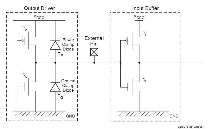
XC5VLX85T-2FFG1136C features: (1)Real 6-input look-up table (LUT) technology; (2)Dual 5-LUT option; (3)Improved reduced-hop routing; (4)64-bit distributed RAM option; (5)SRL32/Dual SRL16 option; (6)Digital Clock Manager (DCM) blocks for zero delay buffering, frequency synthesis, and clock phase shifting; (7)PLL blocks for input jitter filtering, zero delay buffering, frequency synthesis, and phase-matched clock division; (8)True dual-port RAM blocks; (9)Enhanced optional programmable FIFO logic; (10)Built-in optional error-correction circuitry; (11)Optionally program each block as two independent 18-Kbit blocks; (12)1.2 to 3.3V I/O Operation; (13)Source-synchronous interfacing using ChipSync technology; (14)Digitally-controlled impedance (DCI) active termination; (15)Flexible fine-grained I/O banking; (16)High-speed memory interface support; (17)25 x 18, two’s complement, multiplication; (18)Optional adder, subtracter, and accumulator; (19)Optional pipelining; (20)Optional bitwise logical functionality; (21)Dedicated cascade connections; (22)SPI and Parallel FLASH interface; (23)Multi-bitstream support with dedicated fallback reconfiguration logic; (24)Auto bus width detection capability; (25)On-chip/Off-chip thermal monitoring; (26)On-chip/Off-chip power supply monitoring; (27)JTAG access to all monitored quantities.
Diagrams
| Image | Part No | Mfg | Description |  |
Pricing (USD) |
Quantity | ||||||
|---|---|---|---|---|---|---|---|---|---|---|---|---|
 |
 XC5VLX85T-2FFG1136C |
|
IC FPGA VIRTEX-5 85K 1136FBGA |
Data Sheet |
|
|
||||||
| Image | Part No | Mfg | Description | |
Pricing (USD) |
Quantity | ||||||
 |
XC5VFX100T-1FF1136I |
|
IC FPGA VIRTEX-5FXT 1136FFBGA |
Data Sheet |
|
|
||||||
|
XC5VFX100T-1FF1738I |
|
IC FPGA VIRTEX-5FXT 1738FFBGA |
Data Sheet |
|
|
||||||
|
XC5VFX100T-1FFG1136C |
|
IC FPGA VIRTEX 5 100K 1136FFGBGA |
Data Sheet |
|
|
||||||
|
XC5VFX100T-1FFG1136I |
|
IC FPGA VIRTEX 5 100K 1136FFGBGA |
Data Sheet |
|
|
||||||
|
XC5VFX100T-1FFG1738C |
|
IC FPGA VIRTEX 5 100K 1738FFGBGA |
Data Sheet |
|
|
||||||
|
XC5VFX100T-1FFG1738I |
|
IC FPGA VIRTEX 5 100K 1738FFGBGA |
Data Sheet |
|
|
||||||